# SNC8601 Datasheet
High performance cost-effective audio DSP integrating AI algorithm and PMU
# Overview
SNC8601 is optimized for audio DSP applications, with capabilities of low power consumption and cost-effective AI audio algorithm. It supports 24-bit high sampling rate ADC, Tensilica HiFi3 DSP, which can integrate rich AI audio algorithms; Integrates 3 duplex I2S, UAC1.0/2.0 audio service, built-in PMU and rich peripheral interfaces, only need to add a few passive components to provide a complete professional audio AI solution; realize highly integrated, high performance, low BOM cost product.
# Features
# Core and Memory
Cadence® Tensilica® HiFi3 audio DSP @ max. 200MHz
Single-cycle MAC, vector FPU, SIMD
JTAG debug and trace
Proprietary hardware accelerators
256KB IRAM, 256KB DRAM, 48KB cache RAM
On-chip 1MB NOR Flash
One-Time Programmable electrical fuse
# Audio
Two 24-bit audio ADC, SNR>=106dB, with sampling rates: 8, 11.025, 12, 16, 22.05, 24, 32, 44.1, 48, 88.2, 96, 176.4, 192kHz
Two audio ADC line-in supports single-end or differential input
Up to 6 Digital microphone interfaces with programmable DMIC clock frequency and support of low power mode
Automatic Gain/Level Control (AGC) with SNR optimizer
Voice activity detection for low power mode
Programmable Wind Noise Filter (WNF)
Three duplex I2S, sampling rates: 8K~192KHz, max. 32bits
# DSP
Patented noise cancellation for both near-field and far-field
Active echo cancellation
Dereverberation
EQ for audio input/output
Beam forming, DOA
# Power, Clock
Power supply from 3.3V to 5.5V
On-chip ultra-low power management unit
DC-DC regulators and LDOs for all on-chip supply voltages
POR-BOR, overvoltage protection
Always-on domain for ultra-low-power sleep mode
Crystal oscillator @24MHz and 26MHz
On-chip PLL provides all necessary clocks to meet SoC proper operation
# Peripherals
Max. 4 GPIOs
Three duplex I2S, sampling rate 8K~192KHz, max. 32bits
Two I2C master/slave controller
One duplex UART
Tow 12-bit SAR ADC, can be used for headset button detection, battery monitor, or other analog sensor input measurement.
# Applications
Smart TV, Conference System
Multimedia player
Hi-Fi audio system
In-car audio system
# Functional Block Diagram
With a HiFi3 DSP core, on-chip 24-bits/192KSps digital and analog microphone interface, pre-amplifiers, SNC8601 is a truly single-chip solution for high quality audio with low power consumption.
SNC8601 integrates a Cadence HiFi3 core up to 200MHz for system control and digital signal processing, and a high-quality 24-bits/192Ksps Codec with stereo input, 2 analog microphones, and up to 10 digital microphones. It provides up to 512KB zero-wait RAM and a size configurable Flash memory (1MB by default). The on-chip power management unit provides all power supply to meet the on-chip requirements with one power supply. There is one always-on domain to achieve low power consumption. It provides rich peripheral interfaces: three I2S, two I2C, one UART, 4 GPIOs. It supports two auxiliary ADC which can be used for button recognition, analog sensor applications.
SNC8601 provides a powerful digital signal processor to facilitate features and performance for high quality audio applications and products, like automatic echo cancellation, noise cancellation, audio equalization, automatic gain control (AGC), and customized audio effects
# Device Package
| Part Number | Package | Body Size (NOM) |
|---|---|---|
| SNC8601 | BGA 80 | 4.50mm*6.20mm |
# Pin Configuration and Functions
Pin name list with description and ball position:
| Function | Pin name | 80 Ball BGA | Type | Description |
|---|---|---|---|---|
| Xtal Oscillator | XI | D1 | Analog | 24MHz crystal port |
| XO | C1 | Analog | 24MHz crystal port | |
| PMU | VDD_IP33 | J1 | Analog | 3.3V for analog block |
| VDD_IO33 | K1 | Analog | 3.3V for IO | |
| CODEC_VDD | K9 | Analog | 3.3V for Codec | |
| AVDPWR_RAR | K5 | Analog | External power supply | |
| AVDPWR_ESR | K6 | Analog | External power supply | |
| OPM_VOUT | K10 | Analog | Protection LDO output | |
| VDD_CORE11 | K2 | Analog | 1.1V for digital core | |
| ESR_LX | K7 | Analog | DCDC2 switch pin | |
| VSENSE_ESR | K8 | Analog | DCDC2 sense pin | |
| RAR_LX | K4 | Analog | DCDC1 switch pin | |
| VSENSE-RAR | K3 | Analog | DCDC1 sense pin | |
| EFUSE_VDDQ | J7 | Analog | Supply for eFuse | |
| Digital Interface | I2C_CLK | A3 | I/O | I2C interface clock |
| I2C_DAT | B3 | I/O | I2C interface data | |
| GPIO0 | B4 | I/O | I2S1_clk | |
| GPIO1 | B5 | I/O | I2s1_ws | |
| GPIO2 | B6 | I/O | I2s1_sdi | |
| GPIO3 | B7 | I/O | I2s1_sdo | |
| GPIO4 | A4 | I/O | I2s2_clk | |
| GPIO5 | A5 | I/O | I2s2_ws | |
| GPIO6 | A6 | I/O | I2s2_sdi | |
| GPIO7 | A7 | I/O | I2s2_sdo | |
| DMIC_IN1 | A10 | I | DMIC1/2 input (GPIO9) | |
| DMIC_IN2 | A9 | I | DMIC3/4 input | |
| DMIC_IN3 | A8 | I | DMIC5/6 input | |
| DMIC_CLK11 | B10 | O | DMIC1/2 clock (GPIO8) | |
| DMIC_CLK21 | B9 | O | DMIC3/4 clock | |
| DMIC_CLK31 | B8 | O | DMIC5/6 clock | |
| RST_N | J9 | I | Chip reset | |
| GPIOAO | J8 | I | Always-on wake up | |
| UART_TXD | A1 | O | UART TX data | |
| UART_RXD | A2 | I | UART RX data | |
| DFU_N | J10 | I | Firmware update enable | |
| Backup_Boot | B11 | I | For backup boot vector | |
| GPIO10 | J4 | I/O | ||
| GPIO11 | J3 | I/O | ||
| GPIO12 | G2 | I/O | ||
| GPIO13 | F2 | I/O | ||
| GPIO14 | E2 | I/O | ||
| GPIO15 | D2 | I/O | ||
| TEST-EN | C11 | I/O | ||
| Audio Interface | VREG | F12 | Analog | Audio supply |
| VCAP | G12 | Analog | Audio biasing De-cap | |
| AIP1 | A12 | Analog | MIC1 input P port | |
| AIN1 | B12 | Analog | MIC1 input N port | |
| AIP2 | D12 | Analog | MIC2 input N port | |
| AIN2 | C12 | Analog | MIC2 input P port | |
| MICBIAS1 | A11 | Analog | Micbias 1 | |
| MICBIAS2 | E12 | Analog | Micbias 2 | |
| Auxiliary ADC | VINP0_ADC | B1 | Analog | GPADC0 input |
| VINP1_ADC | B2 | Analog | GPADC1 input | GND | VSSA_ADC | C2 | Analog | Analog GND |
| VSSA_USB | H2 | Analog | Analog GND | |
| VSSD | F5678,E5678 | Analog | Digital GND | |
| VSSA_AVS | H11,G11,F11 | Analog | Codec analog GND | |
| AVS_ESR | J6 | Analog | DCDC2 GND | |
| AVS_RAR | J5 | Analog | DCDC1 GND | |
| GNDSENSE | J2 | Analog | All regulator GNDsenses | |
| VSSA_A0 | J11 | Analog | DAC driver GND | |
| VREFN | E11,D11 | Analog | Codec reference GND |
# Specifications
# Absolute Maximum Ratings
| Parameter | Symbol | Min. | Max. | Unit |
|---|---|---|---|---|
| Power | AVDPWR | -0.3 | 5.5 | V |
| AVDD | -0.3 | 3.63 | V | |
| VDD_IP33 | -0.3 | 3.63 | V | |
| VDD_IO33 | -0.3 | 3.63 | V | |
| VDD_OPM | -0.3 | 3.63 | V | |
| VDD_eFuse | -0.3 | 2.75 | V |
# Handling Ratings
| Parameter | Symbol | Min | Max | Unit |
|---|---|---|---|---|
| Ambient Temperature | Ta | -20 | 80 | °C |
| ESD | HBM | -2000 | 2000 | V |
| CMD | -500 | 500 | V |
# Recommended Operating Conditions
| Parameter | Test condition | Min. | Typ. | Max. | Unit | |
|---|---|---|---|---|---|---|
| AVDPWR | Power Supply Voltage range | Referenced to VSS | 3.3 | 5 | 5.5 | V |
| AVDD | Referenced to AVSS | 3.2 | 3.3 | 3.4 | ||
| VDD_IP33 | Referenced to AVSS | 3.2 | 3.3 | 3.4 | ||
| VDD_IO33 | Referenced to IOVSS | 3.2 | 3.3 | 3.4 | ||
| DVDD | Referenced to DVSS | 1.05 | 1.1 | 1.15 | ||
| Main Clock | - | 12 | 13 | MHz | ||
| I2C SCL Clock Frequency | Full Speed | - | 100 | 400 | KHz | |
| Analog input maximum signal range | Full Scale, Gain GID* = 0 dB, boost gain GIM* = 0 dB | 0 | 0.53 | 2.12 | Vpeak | |
| Output load resistace (Rl) | Differential configuration | 16 | Ω | |||
| Output load capacitance | 200 | pF | ||||
| Operating Temperature | -20 | 80 | °C | |||
# Electrical Characteristics, Audio ADC inputs
| Condition: - 40°C to +100°C, AVDD=3.3Vm DVDD=1.1V. Input sine wave with a frequency of 1 kHz, measurement bandwidth 20 Hz - Fs/2 for Fs < 48 kHz, measurement bandwidth 20 Hz - 20 kHz for Fs = 48 kHz to 192 kHz, normal mode, capacitor-less input configuration, unless otherwise specified. | |||||
| Parameter | Test condition | Min. | Typ. | Max. | Unit |
|---|---|---|---|---|---|
| Input level | Full Scale, Gain GID* = 0 dB, boost gain GIM* = 0 dB | 2.12 | Vpp | ||
| Full Scale, Gain GID* = 0 dB, boost gain GIM* = 20 dB | 0.212 | Vpp | |||
| THD+N | 1 kHz sine wave @ Full Scale -3 dB and gain GID* = 0 dB, boost gain GIM* = 0 dB, normal mode and low power mode | 88 | dB | ||
| Dynamic Range | A-weighted, 1 kHz sine wave, normal mode | 106.5 | dB | ||
| A-weighted, 1 kHz sine wave, low power mode | 103.5 | dB | |||
| SNR | A-weighted, 1 kHz sine wave, with activation of the SNR optimizer feature | 106 | dB | ||
| A-weighted, 1 kHz sine wave, gain GID* = 0 dB, boost gain GIM* = 0 dB, normal mode | 94.5 | dB | |||
| A-weighted, 1 kHz sine wave, gain GID* = 0 dB, boost gain GIM* = 0 dB, low power mode | 90.5 | dB | |||
| PSRR | 100 mVpp 1 kHz sinewave is applied to AVD, input data is 0 and gain GID* = 0 dB, boost gain GIM* = 0 dB | 90 | dB | ||
| Input referred noise | A-weighted, 1 kHz sine wave @ Full Scale and gain GID* = 0 dB, boost gain GIM* = 20 dB, normal mode | 3.6 | uVrms | ||
| A-weighted, 1 kHz sine wave @ Full Scale and gain GID* = 0 dB, boost gain GIM* = 20 dB, low power mode | 5 | uVrms | |||
| Channel separation | 1 kHz sine wave @ Full Scale on one channel, no signal on the other channel and gain GID* = 0 dB, boost gain GIM* = 0 dB | 108 | dB | ||
| Inter-channel phase mismatch | 1 kHz sine wave @ Full Scale on two channels and gain GID* = 0 dB, boost gain GIM* = 0 dB, input bypass capacitor inter-channel mismatch = 10% max, master mode | 0.1 | ° | ||
| Gain range | Boost gain GIM* when activated | -2 | 24 | dB | |
| Digital gain GID* | -64 | 63 | dB | ||
| Gain step | GIM* @1kHz | 2 | dB | ||
| GID* @1kHz | 1 | dB | |||
| Gain accuracy | GIM* @1kHz | -1 | 1 | dB | |
| GID* @1kHz | -0.5 | 0.5 | dB | ||
| Input impedance (differential configuration) | Boost gain GIM* = 20 dB Includes 10 pF for ESD, bonding and package pins capacitances | 20 | pF | ||
| Input impedance (single-ended configuration) | Boost gain GIM* = 20 dB Includes 10 pF for ESD, bonding and package pins capacitances | 20 | pF | ||
| Polarity | AIP*-AIN* to DIL/R | 1 | |||
# Electrical Characteristics, Analog Microphone Interface
| Condition: - 20°C to +80°C, AVDD=3.3Vm DVDD=1.1V. Input sine wave with a frequency of 1 kHz, measurement bandwidth 20 Hz - Fs/2 for Fs \< 48 kHz, measurement bandwidth 20 Hz - 20 kHz for Fs = 48 kHz to 192 kHz, normal mode | |||||
| Parameter | Test conditions | Min. | Typ | Max. | Unit |
|---|---|---|---|---|---|
| Micbias ouput level | 2.5 | V | |||
| Micbias output current Current per MICBIAS output | 2 | mA | |||
| Micbias output current Total current for all MICBIAS outputs | 4 | mA | |||
| VREG output level | 2.35 | 2.5 | 2.65 | V | |
| VCAP output level | 1.9 | 2 | 2.1 | V | |
# Digital microphone interface to decimating filter output path
| Condition: Input sine wave with a frequency of 1 kHz, MCLK = 12 MHz or 13 MHz, DMIC_CLK = Fmclk/4, measurement bandwidth 20 Hz - Fs/2 for Fs = 8 to 32 kHz, measurement bandwidth 20 Hz - 20 kHz for Fs = 44.1 kHz to 192 kHz, unless otherwise specified. | |||||
| Parameter | Test condition | Min. | Typ. | Max. | Unit |
|---|---|---|---|---|---|
| Input level | Full Scale max value, Gain GID* = 0 dB | 85.6 | % | ||
| Full Scale min value, Gain GID* = 0 dB | 14.4 | % | |||
| SNR | A-weighted,1kHz sinewave @Full Scale and gain GIDL, GIDR = 0 dB | 100 | dB | ||
| Dynamic Range | A-weighted, 1 kHz sine wave @ Full Scale -60 dB and gain GID* = 0 dB | 100 | dB | ||
| THD+N | 1kHz sinewave @Full Scale-1dB and gain GIDL, GIDR = 0 dB | 90 | dB | ||
| Digital gain | Gain GID* when activated | -64 | 63 | dB | |
| Gain step | GID* @1 kHz | 1 | dB | ||
| Gain accuracy | GID* @1 kHz | -0.25 | 1 | 0.25 | dB |
# Voice detection on digital microphone interface
| Parameter | Test condition | Min. | Typ. | Max. | Unit |
|---|---|---|---|---|---|
| Detection Latency | Detection results based on MIWOK≠CTM r1.0, Far-Field configuration, Power Level Sensitivity set to 5 dB, within 60% truncation of the first phoneme | 25.7 | ms | ||
| VDV (Voice Detected as Voice) | 93.5 | % | |||
| NDV (Noise Detected as Voice) | 7 | % | |||
| VTE (Voice Trigger Efficiency) | 93.25 | % | |||
| Detection Latency | Detection results based on MIWOK≠CTM r1.0, Far-Field configuration, Power Level Sensitivity set to 5 dB, within 60% truncation of the first phoneme | 25.7 | ms | ||
| VDV (Voice Detected as Voice) | 98.5 | % | |||
| NDV (Noise Detected as Voice) | 7 | % | |||
| VTE (Voice Trigger Efficiency) | 95.75 | % | |||
| VDV (Voice Detected as Voice) | Detection results based on MIWOK≠CTM r1.0, Far-Field configuration, Power Level Sensitivity set to 5 dB, within the word length | 100 | % | ||
| Minimum Absolute Detection Threshold | -80 | dBFS | |||
| Power Level Sensitivity | 0 | 31 | dB | ||
| Power Level Sensitivity programmable step | 1 | dB |
# Electrical Characteristics, LDO
| Parameter | Test condition | Min. | Typ. | Max. | Unit |
|---|---|---|---|---|---|
| Operating Temperrature | Junction temperature | -40 | 100 | °C | |
| Input voltage Range, VAVDPWR | 2.7 | 5.5 | V | ||
| Output voltage | 3.3 | V | |||
| Output voltage Accuracy | ±3 | % | |||
| Maximum Output Current,IMAX | 100 | mA | |||
| Dropout voltage,VDROPOUT | IOUT =IMAX | 380 | mV | ||
| PSRR(Power Supply Rejection Ratio) | @ DC | -45 | -30 | dB | |
| no-load current | ILOAD= 0 mA | 40 | uA |
# System Block Diagram

# Theory of Operation
# DSP core
A powerful Cadence HiFi3 DSP core handles system control and audio digital signal processing. Following figure shows the HiFi3 architecture.
The following table shows the key features and configuration of the HiFi3 DSP core:
| Item | Specification | Comment |
|---|---|---|
| Core | Cadence HiFi3 | |
| 32 bit instruction | As system controller and audio signal processing | |
| Processor Clock | Up to 200 MHz | |
| MAC | Single-cycle MAC | |
| FPU | Vector FPU, half-precision | |
| SIMD | Full type of operation | |
| MIPS | 600 MIPS max | 3 slots in HiFi3 |
| I-RAM | 256KB | Local zero-wait RAM for instruction |
| D-RAM | 256KB | Local zero-wait RAM for data |
| I-Cache | 16 KB | 4 cache way, 64 Byte cache line |
| D-Cache | 32 KB | 4 cache way, 64 Byte cache line |
| Bus protocol | AHB-lite | 32-bit data width |
| Timer | 3 timers |
# Interrupt description
HiFi3 supports 32 interrupts which are listed in the following table with priority, where higher-level number means higher priority.
| Configurable IRQ Num | Function | Interrupt (default) | Priority | Comments |
|---|---|---|---|---|
| 0 | USB IRQ | USB | 4 | |
| 1 | USBDMA | 4 | ||
| 2 | ADC | CODEC_IRQADC12 | 4 | ADC DMIC1/2 or AMIC1/2 interrupt |
| 3 | CODEC_IRQADC34 | 4 | ADC DMIC3/4 interrupt | |
| 4 | CODEC_IRQADC56 | 4 | ADC DMIC5/6 interrupt | |
| 5 | CODEC_IRQADC78 | 4 | ADC DMIC7/8 interrupt | |
| 6 | CODEC_IRQADC9A | 4 | ADC DMIC9/A interrupt | |
| 7 | DAC | CODEC_IRQDAC | 4 | DAC interrupt |
| 8 | SW interrupt_0 | SOFTWARE_INT_0 | 4 | SW interrupt 0 |
| 9 | I2S-1 | I2S-1 IRQ | 4 | I2S-1 word clock interrupt |
| 10 | I2S-2 | I2S-2 IRQ | 4 | I2S-2 word clock interrupt |
| 11 | I2S-3 | I2S-3 IRQ | 4 | I2S-3 word clock interrupt |
| 12 | DMAC | DMAC-IRQ | 4 | DMAC interrupt |
| 13 | Maestro (PMU) | Maestro-IRQ | 4 | Maestro interrupt |
| 14 | Codec | Codec-IRQ | 4 | Codec interrupt on AIAS lock event and headphone output short-circuit detection |
| 15 | Codec-IRQ-WT | 4 | Codec interrupt for VAD | |
| 16 | I2C-1 | I2C-1 IRQ | 3 | I2C-1 IRQ |
| 17 | I2C-2 | I2C-2 IRQ | 3 | I2C-2 IRQ |
| 18 | UART | UART IRQ | 3 | |
| Timer | Timer0-IRQ | 3 | Hifi3 own timer | |
| 19 | GPIO678 | GPIO6-IRQ | 3 | Group to one IRQ |
| GPIO7-IRQ | 3 | |||
| GPIO8-IRQ | 3 | |||
| 20 | RTC | RTC-IRQ | 2 | RTC interrupt |
| 21 | Watchdog | Watchdog-IRQ | 2 | watchdog interrupt (32KHz) |
| 22 | GPIO9ABCDEF | GPIO9-IRQ | 2 | Group to one IRQ |
| GPIO10-IRQ | 2 | |||
| GPIO11-IRQ | 2 | |||
| GPIO12-IRQ | 2 | |||
| GPIO13-IRQ | 2 | |||
| GPIO14-IRQ | 2 | |||
| GPIO15-IRQ | 2 | |||
| 23 | USB_Sleep | USB_Sleep_IRQ | 1 | USB skep mode |
| DSP SW interrupt | DSP_SW_IRQ | 1 | Software IRQ from HiFi3 | |
| Timer | Timer1-IRQ | 1 | Hii3 own timer | |
| Trmer2-IRQ | 1 | Hifi3 own timer | ||
| 24 | ADC | ADC-IRQ | 1 | ADC IRQ with eoc signal |
| 25 | PWM Interrupt | PWM_IRQ | 1 | PWM Interrupt |
| 26 | SW interrupt_1 | SOFTWARE_INT_1 | 1 | SW interrupt 1 |
| Profiling | Profing_IRQ | 1 | Profing interrupt |
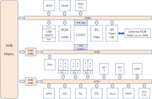
# System bus structure
The following figure shows the multi-layer bus matrix: HiFi3, DMA are masters, while ROM, SPI Flash controller, Codec data, BQ filter, and peripherals are slaves. IRAM and DRAM are TCM type SRAM with 1 cycle operation. 64KB ROM is used for system boot. The Hardware BQ filter is connected on the AHB bus.
AHB and AHP peripherals:
# Data processing flow
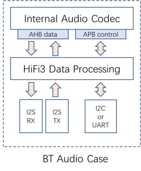
Following figure shows the I2S data flow with the HiFi3 core. This is the application case for Bluetooth headset and beamforming voice command products.
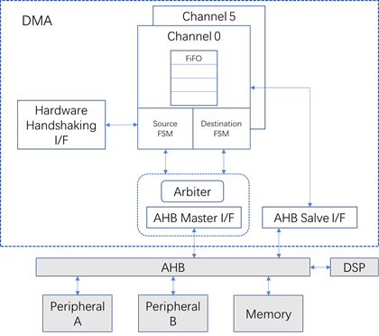
# DMA
DMA controller is connected to the AHB bus. Data are transferred between RAM, Flash controller, and I2S through the DMA controller. The following figure shows the DMA function implementation.

DMA is an AHB-Central DMA Controller core that transfers data from a source peripheral to a destination peripheral over one or more AHB bus, which consists of:
DMA hardware request interface
Up to six channels
FIFO per channel for source and destination
Arbiter
AHB master interface
AHB slave interface
The following figure shows the DMA block diagram:
# Startup, Initialization, and Power
One single power supply can come from Li-ion battery. The on-chip Power Management Unit (PMU) provides all necessary supply voltage to all functional blocks with low power consumption.
Codec module can provide MIC bias for external microphones, 2.5V LDO for audio analog output. PMU supports power-on-reset (POR), brown-out-detect (BOD), and OVP/OCP/ULP protection. PMU can be set via APB bus to work in active mode, sleep mode, and power-down mode.
The following figure shows the power tree architecture, includes:
Single power input from 3.3V to 5.5V
One DC-DC regulator for Core and digital: 1.1V
One Always-on ultra-low-power LDO for sleep-mode: 1.1V
One DC-DC regulator for Codec analog part: 3.3V
One LDO generate 3.3V power for other analog parts
One LDO generate 3.3V power for digital IO
# Power-Up Sequence
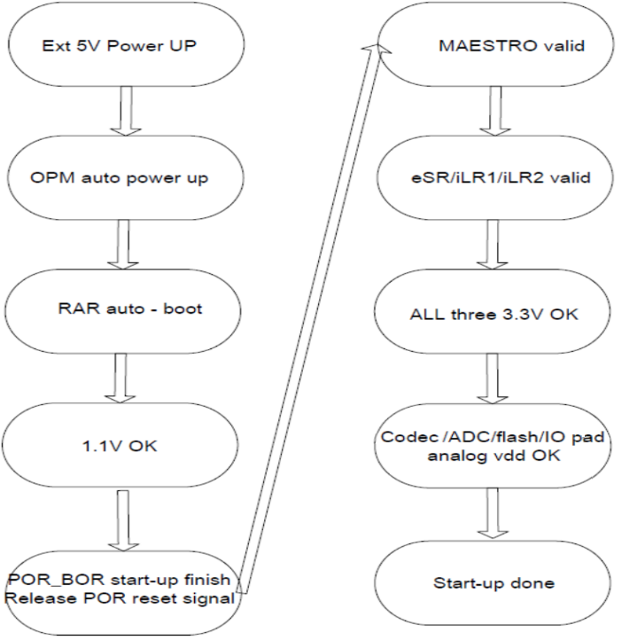
The startup sequence is described in above figure. POR sends out the general reset signal, and Maestro sets all regulators into the right states.
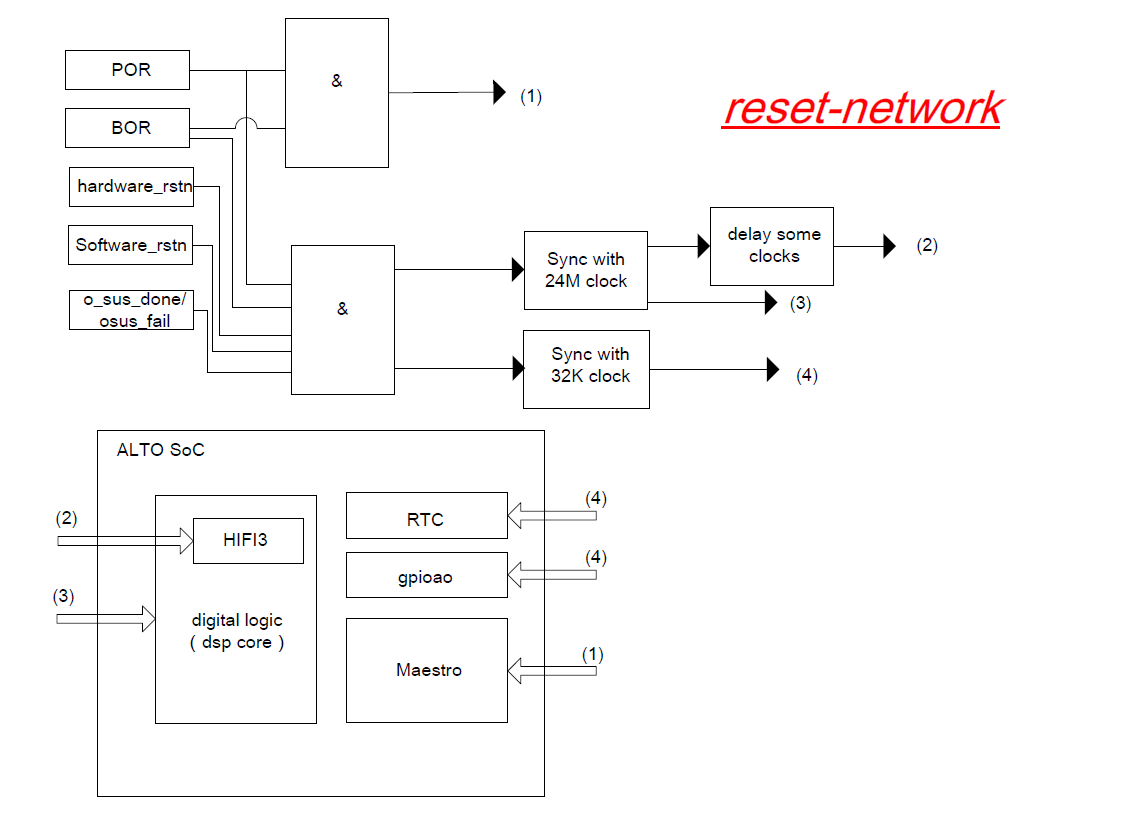
# Reset Network
The following figure shows reset network. There are 4 kinds of reset signal from different function blocks. Reset 1 is generated by POR and BOR, the other 3 kinds of reset signal may come from POR/BOR, hardware reset, software reset, o_sus_done or o_sus_fail.
# Audio Codec
Audio codec includes the following function blocks:
One stereo Analog to Digital Converter (ADC) and additional analog circuit:
Two single-ended or differential analog inputs with boost gain, which can be used either for line-in or mic-in application in capless configuration
- The two-stage gain for record path: an analog boost gain from -2 dB to +24 dB with 2 dB step and a digitally programmable gain from -64 to +63 dB with 1 dB step.
- Ten mono or five stereo digital microphone interfaces with programmable DMIC clock frequency.
Built-in power regulation:
- One low noise linear voltage regulator to supply part of the analog circuits.
- Two microphone biasing outputs for driving up to two microphones.
Signal processing function:
- An Automatic Gain/Level Control (AGC) enables a self-adaptive recording of the sound level during recording.
- A Wind Noise Filter (WNF), a programmable high pass filter feature enabling to reduce wind noise during recording in a windy environment or an open window vehicle.
- A digital WhisperTrigger for digital microphones which wake-up the chip when voice activity is detected.
- An Audio Interface Adaptive Synchronizer (AIAS) system enables to synchronize automatically the input data if the mean sample frequency is close to a standardized value (up to 3% difference).
Its main features include:
- One stereo 24-bit/192Ksps ADC
- Low BOM capacitor-less input
- Up to 6 digital microphone interfaces with programmable DMIC clock frequency and support of low power mode
- 24 to 16-bit signed linear PCM format, support sampling rate of 8, 11.025, 12, 16, 22.05, 24, 32, 44.1, 48, 88.2, 96, 176.4, 192kHz
- Embedded low noise linear regulator for high resilience to power supply noise
- Low power operating mode on the ADC path
- Reduction of audible glitches systems:
- Soft mute mode
- Zero-crossing gain change
- Automatic Gain/Level Control (AGC) with SNR optimizer feature
- Programmable Wind Noise Filter (WNF)
- WhisperTrigger, voice activity detection for digital microphone
- Slave mode interface on ADC with AIAS automatic data rate synchronization
# Clocking and Sampling Rates
# Clock Generation and Management
 The above figure shows crystal oscillator circuit and crystal equivalent circuit. Only the crystal (XTAL) and the capacitances CX1 and CX2 need to be connected externally on XTAL-In and XTAL-Out. The oscillator has also a bypass mode that an external clock is connected directly to the XTAL-In pin.
To get the best performance, it's very critical to select a matching crystal for on-chip oscillator. The load capacitance CL, series resistance Rs, and drive level DL are important parameters to consider while choosing the crystal. Rf is the feedback resistor for the crystal to start oscillation. After selecting the proper crystal, the external load capacitor CX1 and CX2 values can be generally calculated by the following equation:
CX1=CX2= CL -- (Cpad + Cparasitic)
Where:
CL:Crystal load capacitance per terminal
Cpad: Pad capacitance of the XTAL-In and XTAL-Out pins
Cparasitic: Parasitic or stray capacitance of the external circuit.
Following table lists the electrical characteristics of the crystal oscillator:
| Description | Symbol | Min. | Typ. | Max. | Unit |
|---|---|---|---|---|---|
| Frequency range (crystal mode) | Fref | 24 | MHz | ||
| Frequency range (bypass mode) | Fref | 24 | MHz | ||
| Frequency accuracy | -20 | 20 | ppm | ||
| Cycle-to-cycle Jitter | CCJ | -10 | 10 | ps | |
| Output Duty Cycle | t-do | 40 | 50 | 60 | % |
| Equivalent Series Resistance | 40 | Ω | |||
| CL | 8 | pF | |||
| Rf | 1 | MΩ | |||
| Total Power (unloaded) | IDD | TBD | mA |
# Core Clock
The clock generation module includes PLL which generates clock to HiFi3 Core, Codec, I2S, SPI, and other interfaces.
There are two reference oscillators. An on-chip 32kHz RC oscillator is used during power-up and low power mode. An external 24MHz crystal oscillator provides reference clocks in active mode.
Codec master clock is 12MHz, the system clock can be up to 200MHz.

Following table lists clock requirements:
| Clock | Active mode (max MHz) | Sleep mode (MHz) | Duty-cycle |
|---|---|---|---|
| CPU/AHB | 200 | 0 | 45%-55% |
| APB1 | 50 | 0 | 45%-55% |
| APB2 | 100 | 0 | |
| Flash | 108 | 0 | 45%-55% |
| JTAG | External | 0 | 45%-55% |
| Codec | 12 | 0 | 45%-55% |
| USB | 24 | 0 | 45%-55% |
| I2S | 24 | 0 | 45%-55% |
| PLL ref clk | 24 | 0 | 45%-55% |
# Sampling Rates
Sampling frequency and main clock frequency:
| Parameter | Description | Min. | Typ. | Max. | Unit |
|---|---|---|---|---|---|
| Fs | Sampling frequency in normal mode | 8 | 192 | kHz | |
| Fs | Sampling frequency in low power consumption mode (ADC only) | 8 | 16 | kHz | |
| Fmclk | Main clock frequency | 12 or 13 | MHz | ||
| Dmclk | Main clock duty cycle | 0.45 | 0.5 | 0.55 | - |
The relation between MCLK, DMIC_CLK frequencies, and available Fs:
| Clock division ratio (DMIC_RATE) | DMIC-CLK: frequency (Fdmic≠clk) for Fmclk=12Mhz | DMIC-CLK: frequency (Fdmic≠clk) for Fmclk=13Mhz | Available Fs (kHz) |
|---|---|---|---|
| 16 | 750 kHz | 812.5 kHz | 8, 11.025, 12, 16 |
| 12 | 1 MHz | 1.08 MHz | 8, 11.025, 12, 16 |
| 5 | 2.4 MHz | 2.6 MHz | 8, 11.025, 12, 16, 22.05, 24, 32, 44.1, 48, 88.2, 96, 176.4, 192 |
| 4 | 3.0 MHz | 3.25 MHz | 8, 11.025, 12, 16, 22.05, 24, 32, 44.1, 48, 88.2, 96, 176.4, 192 |
# PLL
The following figure shows the PLL architecture where the typical reference clock is 24MHz.
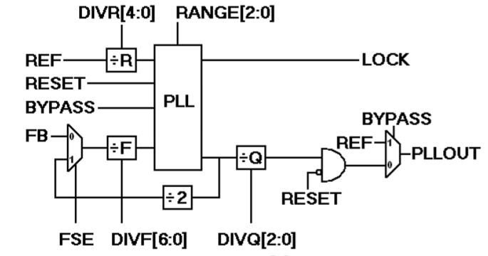
Following table lists the signals for PLL operation:
| Signal | Usage | Limitation |
|---|---|---|
| DIVR[4:0] | Reference Divider Value (binary value + 1 : 00000 = ÷1) | Both REF and post-divide REF must be within the specified range |
| DIVF[6:0] | Feedback Divider Value (binary value + 1 : 0000000 = ÷1) | VCO must be within the specified range |
| DIVQ[2:0] | Output Divider Value (2^ binary value) 001 = ÷2 100 = ÷16 010 = ÷4 101 = ÷32 011 = ÷8 110 = ÷64 | |
| FSE | Chooses between internal and external input paths: 0 = FB pin input 1 = internal feedback | |
| RANGE [2:0] | PLL Filter Range 000=BYPASS 100=26-42MHz 001=Reserved 101=42-68MHz 010=10-16MHz 110=68-110MHz 011=16-26MHz 111=110-200MH | This sets the PLL loop filter to work with the post-reference divider frequency. Choose the highest valid range for best jitter performance, or optimize with post-silicon characterization. |
Following table lists PLL key parameters:
| Description | Symbol | Min. | Typ. | Max. | Unit |
|---|---|---|---|---|---|
| Input Frequency | Fref | 24 | MHz | ||
| VCO Frequency | Fvco | 1000 | 2000 | MHz | |
| Output Frequency | Fout | 20 | 1000 | MHz | |
| Output Duty Cycle | t-do | 45 | 55 | % | |
| Maximum Lock Time | t-lock | 50 | µs | ||
| Reset Time | t-reset | 1 | µs | ||
| Maximum Long Term Jitter | LTJ | ±1% Divided-Ref Period | |||
| Maximum Cycle to Cycle Jitter | CCJ | ±1% Output Period | |||
| Total Power (unloaded) | IDD | 2 | mA | ||
# Control Ports
# I2C/UART
| Item | Quantity | Unit | Specification | Comment |
|---|---|---|---|---|
| UART | 1 | bps | Up to 3M | TX and RX |
| I2C | 2 | kbps | Up to 400K |
# I2S
There are three I2S interfaces, which are specified in the following table.
| Item | Unit | Specification | Comment |
|---|---|---|---|
| Interface number | 3 I2S interface, with word clock, bit clock, data-in, data-out | ||
| Word clock | kHz | Up to 192 | 8, 16, 32, 44.1, 48, 88.2, 96, 176.4, 192 |
| Data width | bits | 16/20/24 | |
| Format | Standard, left-justified, right-justified |
I2S pins are GPIO reusable pins. GPIO mappings are described in the following table, where CLK is the bit clock, WS is the word clock, SDI is the input data, SDO is the output data.
| I2S-1 | I2S-2 | I2S-3 | |||
|---|---|---|---|---|---|
| I2S1_clk | GPIO0 | I2S2_clk | GPIO4 | I2S3_clk | GPIO12 |
| I2S1_ws | GPIO1 | I2S2_ws | GPIO5 | I2S3_ws | GPIO13 |
| I2S1_sdi | GPIO2 | I2S2_sdi | GPIO6 | I2S3_sdi | GPIO14 |
| I2S1_sdo | GPIO3 | I2S2_sdo | GPIO7 | I2S3_sdo | GPIO15 |
# Auxiliary ADC (SAR ADC)
Two 12-bit SAR ADC can be used for headset button detection, battery monitor, or other analog sensor input measurement.
| Parameters | Min. | Typ. | Max. | Unit |
|---|---|---|---|---|
| Resolution | 12 | Bits | ||
| ENOB | 11 | Bits | ||
| Sampling rate | 5 | Msps | ||
| Channel | TBD | |||
| AVDD-aux-ADC | 3.3 | V | ||
| DVDD-aux-ADC | 1.1 | V | ||
| Input voltage range | 0 | 3.3 | V | |
| INL accuracy | -2 | 2 | LSB | |
| DNL accuracy | -1 | 1 | LSB | |
| Offset | -2 | 2 | LSB | |
| Gain error | -1 | 1 | % | |
| Hardware conversion time | 1 | us |
# eFuse
There is one OTP memory of 256-bits which is organized as 32-bit by 8. This is a one-time programmable electrical fuse with random access interface. The electrical fuse is a type of non-volatile memory which can be fabricated in standard CMOS logic process.
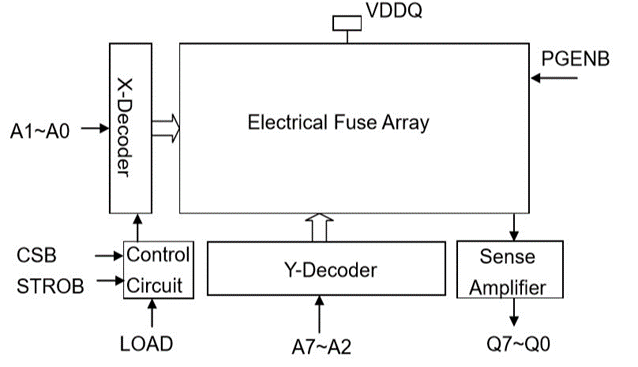
| Pin name | Signal type | Description |
|---|---|---|
| CSB | Input | Active-low chip select in low power standby mode |
| STROBE | Input | High to turn ‘ON’ the array for read or program access |
| LOAD | Input | High to turn ‘ON’ sense amplifier and load data into latch |
| Q7~Q0 | Output | Data output |
| VDDQ | Input | High voltage for fuse programming, ground for read |
| A7~A0 | Input | Address pins |
| PGENB | Input | Program enable (active low) |
| VDD | Supply | Core supply voltage |
| VSS | Supply | Ground |
Key features:
Programming condition:
VDDQ: 2.5V±10%
VDD: 1.1V±10%
Temperature: 125℃~-40℃
Program time: 10us±1us
Read condition:
VDDQ: 0V or floating
VDD: 0.81V~1.21V
Temperature: 125℃~ -40℃
Asynchronous signal interface
# Outline Dimensions
BGA80 dimension information:

# Ordering Guide
Part Number | Type | Package Size | Packing | MoQ |
|---|---|---|---|---|
| SNC8601 | BGA-80L | 4.5mm*6.2mm*1.2mm X: 0.5mm, Y: 0.4mm Pitch | Tape&Reel | 3K |